ASTEC Power Supply - A repair log
If any of your Apple II Power Supplies have any of the RIFA X2 MKT capacitors like the one in the picture on the right, get it replaced as a matter of priority. I didn’t and found out the hard way !
by Mark Cummings
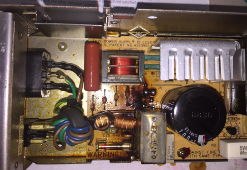
Inside the 240V ASTEC Power Supply before the magic smoke escaped.
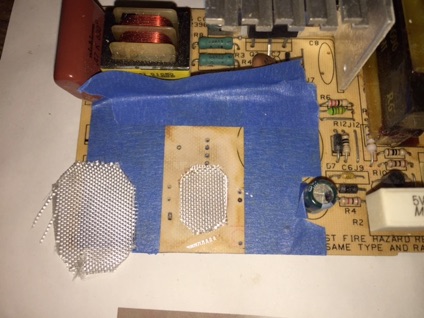
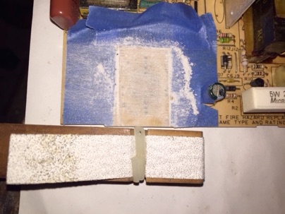
The board prepared ready for ‘glassing’
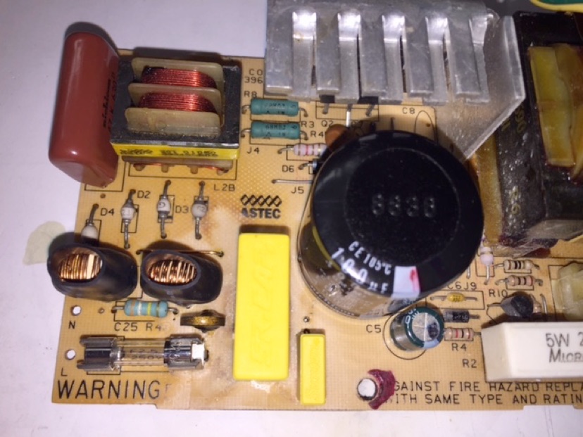
This is how the board looked after a quick clean with IPA.
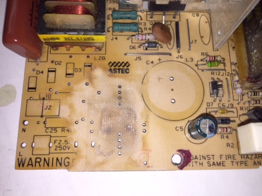
The top of the PCB under C1 is flaking away from the surface.
Observant readers will see a solder ball between D6 and R5 which I missed initially.
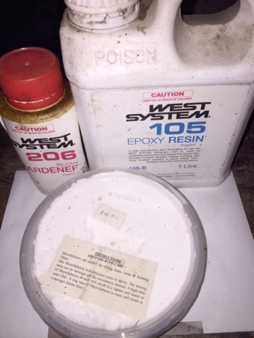
This is the Epoxy I use in Aeromodelling and now PCB repair.
It’s a 5:1 mix instead of 1:1 like a lot of other epoxies.
The West System epoxy is a lot thinner than your standard Araldite or generic brand from the hardware store, but the finish is much harder. I taped up the bottom of the board with masking tape to stop the epoxy going through to the back.
In hindsight I should have soldered all the holes over in the repair area while I did the glassing as some of the resin bled under the tape on the solder side of the board. Next time !
I applied a small amount into the cavity and placed the smaller fiberglass piece, followed by the larger piece on top. Using a skewer, I was able to push the glass down into the epoxy and spread te epoxy up to the edges of the tape. I then placed a small piece of clear acetate sheet (aka. shirt box plastic) on top and made sure I could see the repair through the acetate to ensure it was flat. I then placed a small scrap of 3mm plywood piece on top of the acetate and a couple of pegs on the edges to hold it in place until the epoxy has initially cured. This takes about 30-60 mins. After that I removed the plywood then left it to cure overnight with the acetate left in place. Don’t worry it doesn’t stick to the acetate that well and can be peeled off easily.
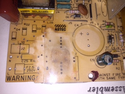
Finished PCB repair ready to refit parts


Back in October 2016 I had a small disaster, which ended up in the magic smoke escaping from my Apple IIGS while I was chatting on IRC A2c.chat an adjacent room. Lucky I was nearby and able to kill the power within a couple of minutes before anything bad happened. Or did I…
Even though I didn’t burn the house down, the smell of burnt toffee was through the house for the next week. Luckily my wife was away at the time.
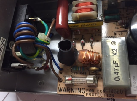
Annoyingly I could have avoided all the grief and repair work if I had replaced the RIFA capacitor when I replaced the faulty electrolytic capacitors 6 months earlier. Unlike most of the electrolytics in the power supply, the X2 cap sits directly across the Active and Neutral.
As you can see from the photo above right, there are no visible signs of a fault with the X2 RIFA capacitor, which is why I didn’t replace it earlier.
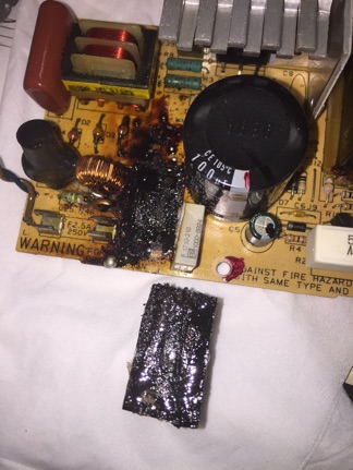
After removing the board and desoldering C1, I could see that the board was badly burnt and not just discoloured on the surface as I had first thought.
From previous PCB repair experience I prefer to use Epoxy resin to repair the board, rather than Polyester resin. Although it’ can be more expensive, I happen to have it already for my Aeromodelling hobby. I mixed up a small batch and mixed in some Micro Balloons to thicken it into more of a paste. The Micro Balloons also makes it lighter and easier to sand.
Before you attempt anything in this article, be aware that you may be exposed to voltages as high as 325VDC, which can be lethal if safety precautions are not taken. If you are not confident or trained you should seek assistance from an electronics technician.
All repairs on the board were carried out after disconnecting power for a minimum of 10 seconds in accordance with manufacturers recommendations.
With the PSU cover removed you can see the damage from C1. Great balls of solder !
A view of the board with C1 removed.
mmm… cooked capacitor any one ?
I did a quick cleanup of the board with IsoPropyl Alcohol (IPA) to inspect the board in detail. This is where I discovered that the top layers of fiberglass in the board under C1 was burnt below the surface, but luckily not through to the solder side where it would have caused severe track damage that would be much more difficult to repair.
PCB Repair Process
I could have left the board as is, installed a new capacitor and left it at that. Electrically it would have been fine, but I think this is worth repairing properly and I have some experience so it shouldn’t be too hard. To repair the board I first had to remove more components to give me enough room for the repair. I then sanded out the damaged areas using a Dremel rotary tool with a ¾” sanding drum and carefully ground off the top layer until most of the burnt part was removed. In some places this was about 1mm - 1.5mm deep. After that I masked some areas off and used a small hobby sanding block with 120 grade Aluminum Oxide sandpaper (that’s how it’s spelt on the back) to feather it into the un-burnt areas. Unfortunately some of the printing will be permanently lost, but it was already burnt, so this is not going to make it worse.
Next I masked off the area that I was going to fill and cut a couple of small pieces of 6oz woven fiberglass cloth. Similar cloth is available from fiberglass suppliers.


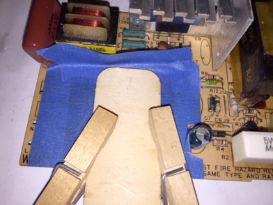
Epoxy and fibreglass applied to board and spread out. Acetate sheet placed on top.
A scrap of 3mm plywood is pegged on top while it sets.
Putting Humpty Dumpty back together again
Once the board repair is done, it’s time to test, clean and refit or replace the original components. This is where I ran into a snag.
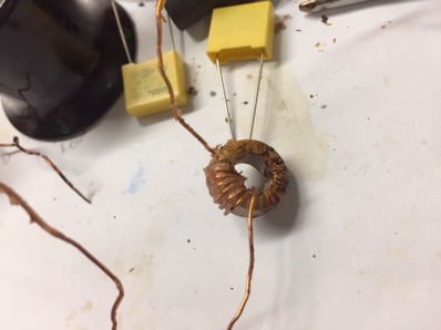
Unlike the inductor L10, which had some heat shrink tubing over it, inductor L9 did not. It got a lot of burnt ‘goop’ in the windings that I was unable to remove without risking damage to the enamel on the wire. It tested OK at 100uH, but looked crusty.
I measured the wire diameter and counted the windings. Jaycar did not have one the same size in their catalogue, nor did they have the ferrite core in that size. But they did have the enameled copper wire, which I purchased. I removed the old wire from the ferrite core and cleaned the core. 48 turns of 0.63mm diameter copper wire later and I had myself a rewound 100uH ‘clean’ inductor. For extra protection and to save repeating this exercise again later I added some black heat shrink over the top the same as L10.
Once the acetate is removed it leaves the fill slightly above the PCB due to the thickness of the masking tape. This is sanded down by masking off the surrounding areas, and about 5mm outside of the lip of the fill. This will prevent further much damage to the top of the board and the printed overlay. Using finer 120grit and 180 grit paper to leave a smooth finish. After that the holes were re-drilled with the correct drill sizes to clear out all the carbon that was still in them.
Hobby sanding block with 80 grit sand paper.
Acetate removed leaving a glossy flat finish.
The only other part that was dead was the fuse, which broke while I was removing it from the holder. All that goo had glued it in place. It’s a 2.5A 250VAc fuse, which fortunately Jaycar carry in stock.
A bit of a delay…
Before I refitted the board I decided to get some scans of the board and kept it out for the last two months while I reverse engineered the circuit board overlay and circuit diagram.
Check back here later for my next article with Circuit Diagram and PCB Overlay.
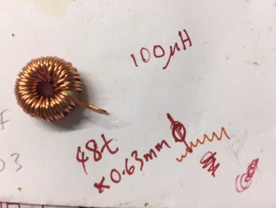
Freshly rewound and clean inductor
100uH inductor L9 with burnt on ‘goop’ between the windings.
Cleaning
I then did a thorough clean on the top and bottom of the board with IsoPropyl Alcohol, then a rinse with detergent and warm water using a very soft bristle artist’s paint brush. After that I blew most of the water off with my air compressor at 40-60 psi, being careful not to blow parts off the board.
I then used my hot air gun set to 50deg C to warm up the whole board and evaporate any remaining moisture. If this is done properly there is no need to wait days for it to dry out, and by blowing the water off, there is far less contaminants left on the board or under the parts. Water isn’t as clean as it looks.
A similar treatment was required for the inside of PSU enclosure, which also suffered a similar fate. I had to remove the power switch before washing because I didn’t want to get water inside the switch. Just plenty of IsoPropyl Alcohol and CO Contact cleaner for that. Lastly a bit of CO contact cleaner sprayed into the spade connectors for the power switch and it was ready to solder back onto the mains wires.
My first tests are without any load connected, just to make sure the voltages are not too high for the Apple IIGS which I am going to connect it to.
The +5V was a bit high at +5.40V but I suspected this would drop once plugged in. After connecting to the IIGS with a CFFA3000 and an AE 4MB GS RAM card the 5V line dropped to 5.04V. Perfect. I took the opportunity to measure a bunch of voltages for the circuit diagram I am working on.
Finally done and ready to install. I also replaced C2 temporarily with a 0.01uF 250VAC X2 capacitor but have since replaced that with the proper Y2 capacitor.
Coming soon...
I have couple more articles on the power supply which are almost finished.
- A Safety modification which can be applied to the IIGS ASTEC and DynaComp Power Supplies.
- The full circuit diagram and PCB Overlay for the IIGS ASTEC supply.
MC