
Another Apple Power Supply reverse engineered. This time it’s for the Apple IIGS ASTEC Power Supply
by Mark Cummings
I must admit I actually finished the bulk of these diagrams three years ago but hadn’t finished all the finer details until recently. This page specifically refers to the 240V version of the power supply which does not have the capability of being jumpered to a 115V version like some of the other Apple ][ power supplies do.
These power supplies were fitted in the 240V ROM1 and ROM3 Apple IIGS’ but there are several minor revisions to the PCB and parts. I had access to REV -02, -03 and -06.
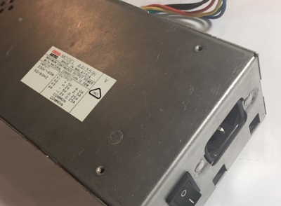
240V ASTEC Power Supply case.
(typically installed in the Apple IIGS)
Before I started this project I searched the internet to see what might already exist. I was lucky to find that there is actually a version of the circuit diagram that was originally authored by Jerzy Sobola back in 2005. This can be found on the appleii-box.de web site. While this diagram was legible I found the layout a bit difficult to follow and there seemed to be some parts missing which I later confirmed.
Circuit Diagram created with Protel Schematic application
The circuit diagram should be legible on an A4 page but if you have access to an A3 printer thats even better. If it’s one thing I hated from my experience reading TV circuit diagrams in the past is that they are often very difficult to read the component values. I have included some DC voltages on the diagram but keep in mind your voltages may vary slightly. Be careful when measuring voltages on the primary side of the circuit as they are with respect to 0 Volts on the primary side.
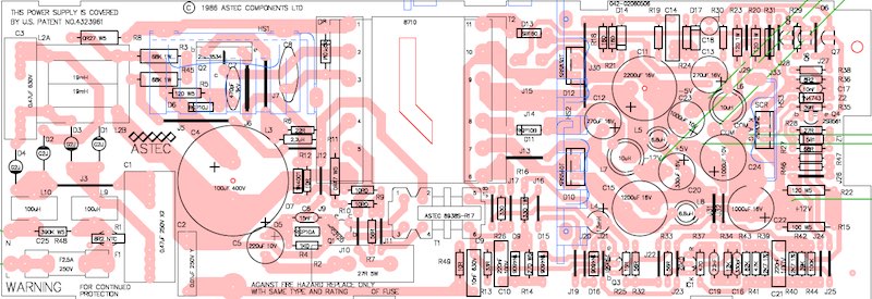
PCB composite overlay generated from Protel PCB Application
Updated diagrams now include plugs and wiring harness
The parts list was originally created from Protel Autotrax, but due to various revisions the list was edited and multiple versions are included in the linked list. The majority of parts should be the same as your power supply but your milage may vary. If you do find errors or other parts in your own power supply please send me the information so I can add it in a later revision. My email is on the circuit diagram.


I hope these diagrams and parts list will be of use if you ever have to work on your power supply.
MC
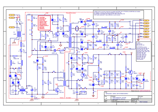
The method I typically use to reverse engineer a circuit is to first draw the PCB overlay in Protel Autotrax and accurately place all the components on the PCB at 1:1 scale. I then print out a mirror image scan of the reverse side of the PCB just showing the tracks. Using that image I then link all the tracks to the parts and adjust track widths to approximately the original size. This is a tedious process but gets faster as you go. Often I have to create new component patterns to match the part. This is especially the case for any unique items like transformers and heat sinks. Once the PCB overlay is drafted I then create a diagram in Protel Schematic using the PCB overlay. After finishing the draft schematic I then print both diagrams out and get a pen out to cross check every single part and node and I often find most of my errors that way. In this case I also had the other diagram from the web to refer to, so I also used that to cross check. Seemingly Jerzy made a lot of errors too, however I found this method invaluable to double check my version of the circuit.
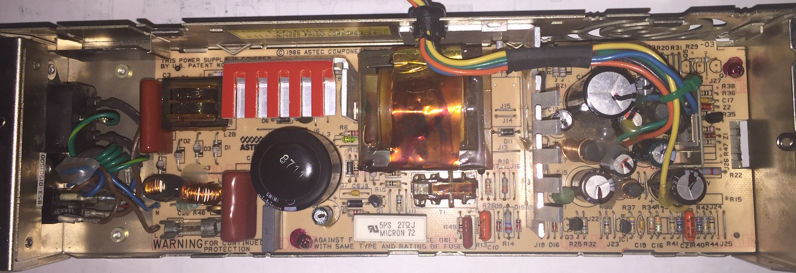
Top view of the PCB after removing from the Apple IIGS.
(The RED paint is a safety modification which I will discuss in another article)

UPDATED 08 Apr 2020
A traditional BW PCB overlay
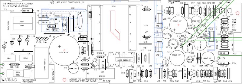
V 2.0
V 2.0
